Your CMP Foundry: Contract Manufacturing and Research & Development
The Entrepix foundry can process your overflow production, provide process engineering solutions and demonstrate equipment performance prior to sales and installation.
Entrepix’ Foundry is home to a variety of wafer production services and R&D that we perform on behalf of our clients. We are here as an extension of your team to assist in device fabrication, volume production, research new processes well as demonstrate and qualify new materials, equipment and consumables.
Engineering and Technology Development for CMP
Entrepix has a knowledgeable team of engineers and technology experts to help clients in CMP, cleaning, and distributed process flows. We work with all wafer diameters from coupons to 200mm, and help our clients:
Rapidly advance technology
Study cost reduction
Integrate new materials
Develop process improvements
Screen consumables
Assess cost and productivity
Achieve flexibility in design and processing methods
Volume Production
We can help build and produce wafers to your needs and specifications for complete outsourcing and as overflow capacity. As a top 10 IDM, we’ve processed more than one million wafers and are ISO 9001:2015 certified.
We offer guaranteed cycle times and use quality systems like FMEAs, SPC, internal audits, and CARs.
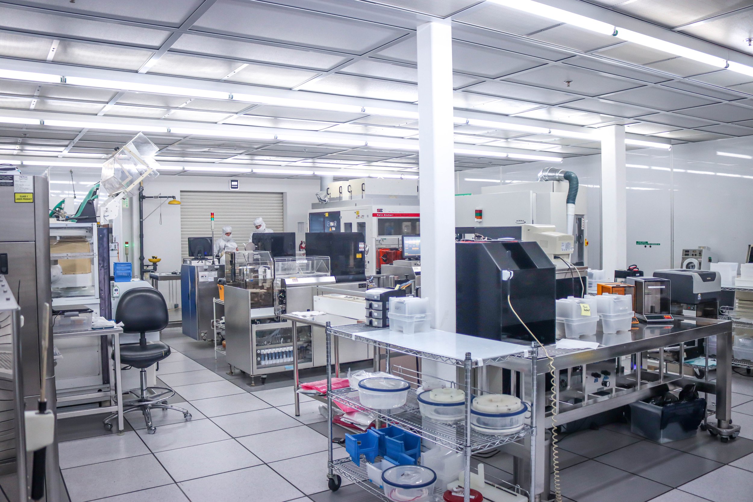
In-House Processing Tool Sets
At Entrepix, we use the following processing tools to meet your success criteria:
| Processing Tools | Platforms |
|---|---|
| CMP | AMAT Mirra: 150-200mm wafer processing |
| IPEC 472(2): Coupon-200mm | |
| Post-CMP Cleans | OnTrak DSS-200 Synergy: 100-200mm |
| OnTrak DSS-200 Series 2: 100-200mm | |
| SRD: 75-200mm |
In-House Metrology Equipment
At Entrepix, we use the following metrology tools to ensure uniformity:
| Metrology Tools | Platforms |
|---|---|
| Dielectric Film Thickness | Thermawave Optiprobe 2600DUV |
| Mikropack UV/Vis/NIR Reflectometer | |
| Conductive Film Thickness | CDE ResMap 168 4-point probe |
| Substrate Thickness | FSM 413-300 |
| Surface Profilometer | Dektak D8 (with ultralow force and 3D mapping) |
| Tencor P2 | |
| Precision Analytical Balance | Mettler-Toledo, A and D, Sartorius |
| Defect Inspection | KLA-Tencor SP1 TBI (200mm) |
| AMAT Orbot WF-736DUO | |
| Defect Review | Leica optical review (built into AMAT platforms) |
| Optical Microscopes | Nikon Optiphot |
| Zeiss Ergoplan (with Nomarski DIC) | |
| Leica stereozoom | |
| Miscellaneous | Various analytical and characterization equipment |
| Also Available (third party) | SEM, AFM, TXRF, and other techniques (additional cost) |
Materials We Polish
CMOS
Oxide
Tungsten
Copper
Barrier metals (Ta, Co, Ru)
Shallow trench
Polysilicon
Low k dielectrics
Capped ultra low k
Metal gates
Gate insulators
High k dielectrics
Ir and Pt electrodes
Refractory metals
Aluminum
Substrate/Epi
Si and SOI
GaAs and AIGaAs
InP and InGaP
Poly-AIN and GaN
CdTe and HGCdTe
Ge and SiGe
Lithium Niobate
Titanium
Quartz, glass, and silica
Sapphire
Diamond and DLC
SiC
New Applications
MEMS
Through Si Vias (TSV)
Direct wafer bond
3D packaging
Ultra thin wafers
Polymers and resists
CNT and nanodevices
NiFe and NiFeCo
Al and stainless steel
Detector arrays
Magnetics
Photonics and solar
LED and optics
Power devices
Analog and RF
FINFET structures
Certifications

Get Assistance with Research and Manufacturing
Need help with research or manufacturing? Contact us and we’ll reply to you shortly.